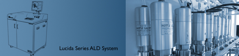
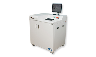
| Atomic layer deposition system for R&D applications |
| Applications |
- Thin film process for ALD research
: Al2O3, HfO2, ZrO2, TiO2, ZnO ……
- 100~200mm wafers
- Applications of R&D
- Very low price
|
| Features |
- ALD ultra-thin high-k dielectric with good thickness
uniformity and 100% conformal step
coverage
- Advanced process kit and small-volume chamber for short cycle times
- Extremely materialize ALD mechanism
(traveling wave method)
- Small foot print
- Totally integrated process module
- Easy process control
- Minimize gas supply line length
|
| Technical specifications |
| Substrate size |
100~200 mm |
| Substrate temperature |
25℃ ~ 350 ℃ (± 0.2 ℃) @ 1Torr, in wafer |
| Precursor sources |
3, heated 2 sources and H2O source |
| Deposition uniformity |
<±2% |
| Footprint |
950 x 700 mm |
| Compatibility |
Clean room class 100 |
| Control system |
PC control base (full auto) |
| Optional |
Up to 4 heated sources |
| Optional |
Lucida cooler(2ch) |
|
|
 |